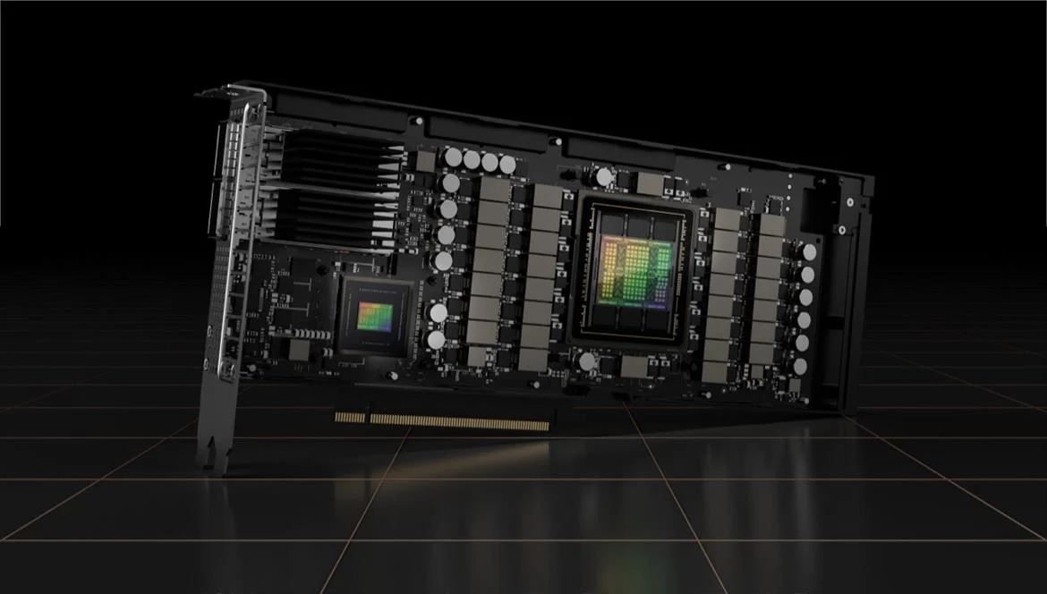
Nvidia’s GPU Technology Conference (GTC) is underway. During CEO Jensen Huang’s keynote, details of Nvidia’s next generation Hopper architecture were revealed. Though it’s an AI and data centre focused GPU, it gives us a few hints of what we can expect from Nvidia’s gaming-oriented Ada Lovelace GPU architecture, which is due for release later in 2022.
The H100 is a major step forward over the current flagship A100. The full GPU contains 80 billion transistors or 26 billion more that the A100. It’s built on a custom TSMC 4nm process. It supports up to 80GB of HBM 3 memory delivering up to 3 TB/s of bandwidth.
The H100 supports PCIe 5.0 and NVLink for connecting multiple GPUs together. It can deliver 2,000 TFLOPS of FP16 and 1,000 TFLOPS of TF32 performance, triple that of the A100. Hopper introduces a new instruction set called DPX. It’s designed to accelerate performance in fields as varied as disease diagnosis, quantum simulation, graph analytics and routing optimizations.
The full H100 GPU includes 18432 CUDA cores and 576 Tensor cores. That compares to the A100 with 8192 and 512 respectively, though for now not all of the cores are unlocked, presumably to maximise yields. The core clocks are also not finalised. Despite being fabricated on such an advanced node, the SXM version of the H100 comes with a TDP of 700W. That’s right, seven. hundred. watts.
The H100 is set to be a monster of a card, but is it relevant to PC gamers? The answer is sort-of. H100 is all about compute performance and not graphics, but we can take some bits of information and use it to predict what the gaming version might look like.
The move to a custom TSMC 4nm node is a major step forward over the Samsung 8nm process used for the RTX-30 series. It’s likely to be used for RTX-40 series cards too. Also noteworthy is support for PCIe 5.0. Though by itself it’s not expected to deliver any real performance benefit over PCIe 4.0, it may well do over PCIe 3.0 which is still widely in use across many gaming systems.

But perhaps the biggest nugget of all is the rather astonishing 700W TDP of the high-end configuration. Just look at the VRM of that card! 700W for a data centre product is something that can be managed, but if we get anything like that for a flagship RTX 4090 then we’d be shocked. Sadly, rumours of steep increases in power consumption continue to surface. Even 500W is a jump and it means that four slot graphics cards may become the norm, at the top end of the market anyway.
Nvidia is still working on the H100. If its main characteristics are shared with the RTX 40 series, it’s fair to say that the high end cards will be hot and power hungry, but packed full of tech and much faster than the RTX 3090 (and the soon to be released RTX 3090 Ti). AMD will compete with its RDNA3 based cards and it’s shaping up to be a hell of a battle, with all out performance clearly being a priority for both companies at the expense of power efficiency. We can’t wait!

